What you should know about ENC28J60 Ethernet Controller before interfacing it?
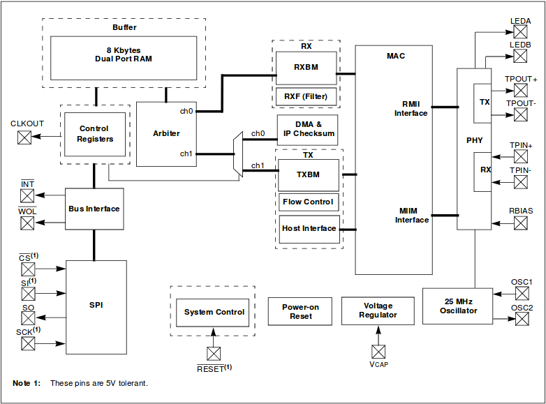
Functional Blocks :
The ENC28J60 is a stand-alone Ethernet controller with an industry standard Serial Peripheral Interface (SPI™). It is designed to serve as an Ethernet network interface for any controller equipped with SPI.
The ENC28J60 consists of seven major functional blocks:
1. An SPI interface that serves as a communication channel between the host controller and the ENC28J60.
2. Control Registers which are used to control and monitor the ENC28J60.
3. A dual port RAM buffer for received and transmitted data packets.
4. An arbiter to control the access to the RAM buffer when requests are made from DMA, transmit and receive blocks.
5. The bus interface that interprets data and commands received via the SPI interface.
6. The MAC (Medium Access Control) module that implements IEEE 802.3 compliant MAC logic.
7. The PHY (Physical Layer) module that encodes and decodes the analog data that is present on the twisted pair interface. The device also contains other support blocks, such as the oscillator, on-chip voltage regulator, level translators to provide 5V tolerant I/Os and system control logic
SERIAL PERIPHERAL INTERFACE (SPI) :
The ENC28J60 is designed to interface directly with the Serial Peripheral Interface (SPI) port available on many micro-controllers. The implementation used on this device supports SPI mode 0,0 only. In addition, the SPI port requires that SCK be at Idle in a low state.
    //SPI MODE 0 0 -> CPOL , CPHA set to 0 0 which is already
    //CPOL : This bit selects the clock polarity when the bus is idle
    //CPHA : This bit determines when the data needs to be sampled.
    // SPI Control Register(SPCR)
    //SPE – (SPI Enable) The SPI Enable bit is used to enable SPI as a whole
    // MSTR – Master/Slave Select This bit is used to configure the device as Master or as Slave
    SPCR = (1<<SPE)|(1<<MSTR);

    //SPI Status Register(SPSR)
    //Set this bit to 1 to enable SPI Double Speed Mode.
    SPSR |= (1<<SPI2X);
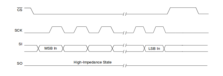
Commands and data are sent to the device via the SI pin, with data being clocked in on the rising edge of SCK.
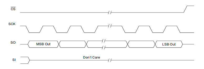
Data is driven out by the ENC28J60 on the SO line, on the falling edge of SCK. The CS pin must be held low while any operation is performed and returned high when finished.
SPI Instruction Set
The operation of the ENC28J60 depends entirely on commands given by an external host controller over the SPI interface. These commands take the form of instructions, of one or more bytes, which are used to access the control memory and Ethernet buffer spaces. At the least, instructions consist of a 3-bit opcode followed by a 5-bit argument that specifies either a register address or a data constant. Write and bit field instructions are also followed by one or more bytes of data. A total of seven instructions are implemented on the ENC28J60.
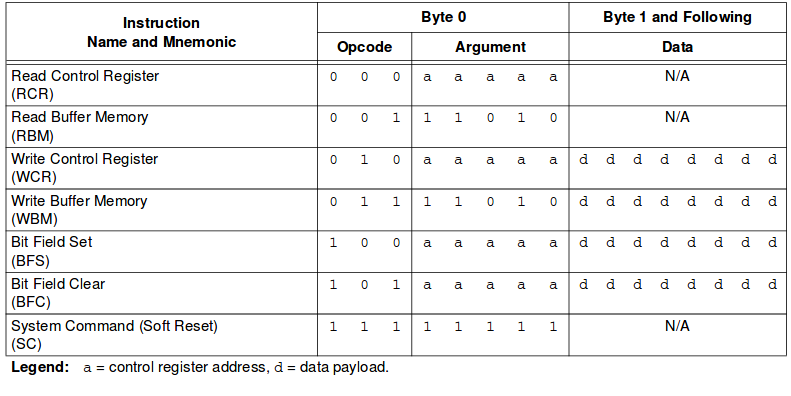
#define ENC28J60_READ_CTRL_REG       0x00
#define ENC28J60_READ_BUF_MEM        0x3A
#define ENC28J60_WRITE_CTRL_REG      0x40
#define ENC28J60_WRITE_BUF_MEM       0x7A
#define ENC28J60_BIT_FIELD_SET       0x80
#define ENC28J60_BIT_FIELD_CLR       0xA0
#define ENC28J60_SOFT_RESET          0xFF

#define ENC28J60_CONTROL_PORT   PORTB
#define ENC28J60_CONTROL_DDR    DDRB
#define ENC28J60_CONTROL_CS     4
// set CS to 0 = active
#define CSACTIVE ENC28J60_CONTROL_PORT&=~(1<<ENC28J60_CONTROL_CS)
// set CS to 1 = passive
#define CSPASSIVE ENC28J60_CONTROL_PORT|=(1<<ENC28J60_CONTROL_CS)
//
#define waitspi() while(!(SPSR&(1<<SPIF)))
//Proper Blank Select Mechanism Should Implement
//Read ControlOperation
void ReadControlRegister(unit8_t address)
{
       CSACTIVE;
        // issue read command
        //address is control register
        SPDR = ENC28J60_READ_CTRL_REG | address;
        waitspi();
        // read data
        SPDR = 0x00;
        waitspi();
        // do dummy read if needed (for mac and mii, see datasheet page 29)
        if(address & 0x80)
        {
                SPDR = 0x00;
                waitspi();
        }
        // release CS
        CSPASSIVE;
        return(SPDR);
}

//Proper Blank Select Mechanism Should Implement
//Write ControlOperation
void WriteControlRegister(uint8_t address, uint8_t data)
{

        CSACTIVE;
        // issue write command
        SPDR = ENC28J60_READ_CTRL_REG | address ;
        waitspi();
        // write data
        SPDR = data;
        waitspi();
        CSPASSIVE;
}

//Write ControlOperation
void BitFieldSet(uint8_t address, uint8_t data)
{

        CSACTIVE;
        // issue write command
        SPDR = ENC28J60_BIT_FIELD_SET | address ;
        waitspi();
        // write data
        SPDR = data;
        waitspi();
        CSPASSIVE;
}
MEMORY ORGANIZATION :
All memory in the ENC28J60 is implemented as static RAM. There are three types of memory in the ENC28J60:
- Control Registers
- Ethernet Buffer
- PHY Registers
The Ethernet buffer contains transmit and receive memory used by the Ethernet controller in a single memory space. The sizes of the memory areas are programmable by the host controller using the SPI interface. The Ethernet buffer memory can only be accessed via the read buffer memory and write buffer memory SPI commands
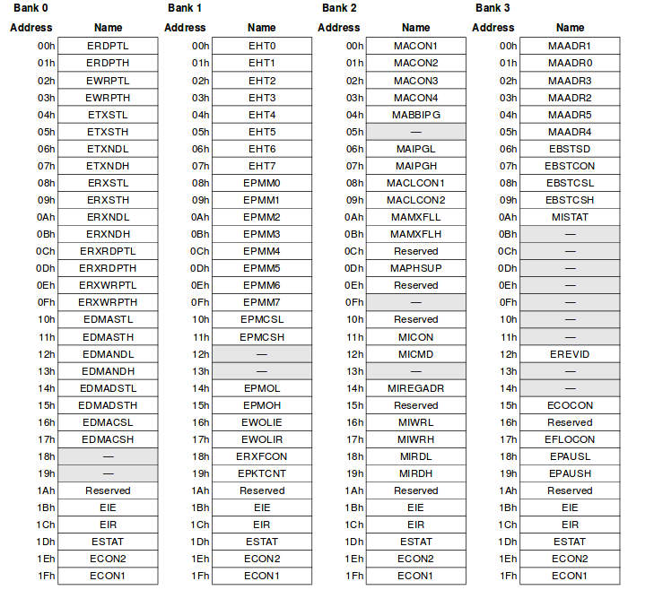
Control Register
The Control Register memory is partitioned into four banks, selectable by the bank select bits BSEL1:BSEL0 in the ECON1 register. Each bank is 32 bytes long and addressed by a 5-bit address value.
The last five locations (1Bh to 1Fh) of all banks point to a common set of registers: EIE, EIR, ESTAT, ECON2 and ECON1. These are key registers used in controlling and monitoring the operation of the device. Their common mapping allows easy access without switching the bank.
INITIALIZATION :
Before the ENC28J60 can be used to transmit and receive packets, certain device settings must be initial- ized. Depending on the application, some configuration options may need to be changed. Normally, these tasks may be accomplished once after Reset and do not need to be changed thereafter
Receive and Transmission Buffer
#define ETXSTL           0x04
#define ETXSTH           0x05
#define ETXNDL           0x06
#define ETXNDH           0x07
#define ERXSTL           0x08
#define ERXSTH           0x09
#define ERXNDL           0x0A
#define ERXNDH           0x0B
#define ERXRDPTL         0x0C
#define ERXRDPTH         0x0D

// The RXSTART_INIT should be zero. See Rev. B4 Silicon Errata
// buffer boundaries applied to internal 8K ram
// the entire available packet buffer space is allocated
//
// start with recbuf at 0/
#define RXSTART_INIT     0x0
// receive buffer end
#define RXSTOP_INIT      (0x1FFF-0x0600-1)
// start TX buffer at 0x1FFF-0x0600, pace for one full ethernet frame (~1500 bytes)
#define TXSTART_INIT     (0x1FFF-0x0600)
// stp TX buffer at end of mem
#define TXSTOP_INIT      0x1FFF

// Rx start
WriteControlRegister(ERXSTL, RXSTART_INIT&0xFF);
WriteControlRegister(ERXSTH, RXSTART_INIT>>8);
// set receive pointer address
WriteControlRegister(ERXRDPTL, RXSTART_INIT&0xFF);
WriteControlRegister(ERXRDPTH, RXSTART_INIT>>8);
// RX end
WriteControlRegister(ERXNDL, RXSTOP_INIT&0xFF);
WriteControlRegister(ERXNDH, RXSTOP_INIT>>8);
// TX start
WriteControlRegister(ETXSTL, TXSTART_INIT&0xFF);
WriteControlRegister(ETXSTH, TXSTART_INIT>>8);
// TX end
WriteControlRegister(ETXNDL, TXSTOP_INIT&0xFF);
WriteControlRegister(ETXNDH, TXSTOP_INIT>>8);
Receive Filters
The appropriate receive filters should be enabled or disabled by writing to the ERXFCON register.
MAC Initialization Settings
#define MACON1           0x00
#define MACON2           0x01
#define MACON3           0x02
#define MABBIPG          0x04
#define MAIPGL           0x06
#define MAIPGH           0x07
#define MAMXFLL          0x0A
#define MAMXFLH          0x0B

#define MAADR1           0x00
#define MAADR0           0x01
#define MAADR3           0x02
#define MAADR2           0x03
#define MAADR5           0x04
#define MAADR4           0x05

#define MACON1_LOOPBK    0x10
#define MACON1_TXPAUS    0x08
#define MACON1_RXPAUS    0x04
#define MACON1_PASSALL   0x02
#define MACON1_MARXEN    0x01

#define MACON3_PADCFG2   0x80
#define MACON3_PADCFG1   0x40
#define MACON3_PADCFG0   0x20
#define MACON3_TXCRCEN   0x10
#define MACON3_PHDRLEN   0x08
#define MACON3_HFRMLEN   0x04
#define MACON3_FRMLNEN   0x02
#define MACON3_FULDPX    0x01

// max frame length which the conroller will accept:
#define        MAX_FRAMELEN        1500        // (note: maximum ethernet frame length would be 1518)

// enable MAC receive
WriteControlRegister(MACON1, MACON1_MARXEN|MACON1_TXPAUS|MACON1_RXPAUS);
// bring MAC out of reset
WriteControlRegister(MACON2, 0x00);
// enable automatic padding to 60bytes and CRC operations
BitFieldSet(MACON3, MACON3_PADCFG0|MACON3_TXCRCEN|MACON3_FRMLNEN);
// set inter-frame gap (non-back-to-back)
WriteControlRegister(MAIPGL, 0x12);
WriteControlRegister(MAIPGH, 0x0C);
// set inter-frame gap (back-to-back)
WriteControlRegister(MABBIPG, 0x12);
// Set the maximum packet size which the controller will accept
// Do not send packets longer than MAX_FRAMELEN:
WriteControlRegister(MAMXFLL, MAX_FRAMELEN&0xFF);
WriteControlRegister(MAMXFLH, MAX_FRAMELEN>>8);

// write MAC address
// NOTE: MAC address in ENC28J60 is byte-backward
WriteControlRegister(MAADR5, macaddr[0]);
WriteControlRegister(MAADR4, macaddr[1]);
WriteControlRegister(MAADR3, macaddr[2]);
WriteControlRegister(MAADR2, macaddr[3]);
WriteControlRegister(MAADR1, macaddr[4]);
WriteControlRegister(MAADR0, macaddr[5]);
PHY Initialization Settings
#define PHCON2           0x10
#define MIREGADR         0x14
#define MIWRL            0x16
#define MIWRH            0x17

#define PHCON2_FRCLINK   0x4000
#define PHCON2_TXDIS     0x2000
#define PHCON2_JABBER    0x0400
#define PHCON2_HDLDIS    0x0100
#define MISTAT           0x0A

#define MISTAT_BUSY      0x01

void enc28j60PhyWrite(uint8_t address, uint16_t data)
{
        // set the PHY register address
        WriteControlRegister(MIREGADR, address);
        // write the PHY data
        WriteControlRegister(MIWRL, data);
        WriteControlRegister(MIWRH, data>>8);
        // wait until the PHY write completes
        while(ReadControlRegister(MISTAT) & MISTAT_BUSY){
                _delay_us(15);
        }
}
enc28j60PhyWrite(PHCON2, PHCON2_HDLDIS);